- 您现在的位置:买卖IC网 > Sheet目录2009 > MAX5101BEUE+ (Maxim Integrated Products)IC DAC 8BIT TRPL R-R 16-TSSOP
MAX5101
+2.7V to +5.5V, Low-Power, Triple, Parallel
8-Bit DAC with Rail-to-Rail Voltage Outputs
2
_______________________________________________________________________________________
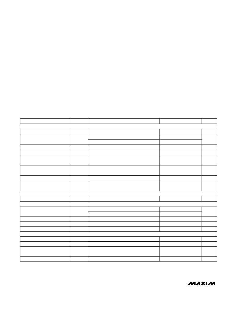
ABSOLUTE MAXIMUM RATINGS
ELECTRICAL CHARACTERISTICS
(VDD = +2.7V to +5.5V, RL = 10k
, CL = 100pF, TA = TMIN to TMAX, unless otherwise noted. Typical values are at VDD = +3V and
TA = +25°C.)
Stresses beyond those listed under “Absolute Maximum Ratings” may cause permanent damage to the device. These are stress ratings only, and functional
operation of the device at these or any other conditions beyond those indicated in the operational sections of the specifications is not implied. Exposure to
absolute maximum rating conditions for extended periods may affect device reliability.
VDD to GND ..............................................................-0.3V to +6V
D_, A_, WR to GND ..................................................-0.3V to +6V
OUT_ to GND ...........................................................-0.3V to VDD
Maximum Current into Any Pin .........................................±50mA
Continuous Power Dissipation (TA = +70°C)
16-Pin TSSOP (derate 5.7mW/°C above +70°C) ..........457mW
Operating Temperature Range
MAX5101_EUE .................................................-40°C to +85°C
Maximum Junction Temperature .....................................+150°C
Storage Temperature Range .............................-65°C to +150°C
Lead Temperature (soldering, 10s) .................................+300°C
Code 00 to code FF hex
MAX5101A
Code 00 to code FF hex
To 1/2LSB, from code 10 to code F0 hex
From code 00 to code F0 hex
VIN = VDD or GND
Code = F0 hex
VDD = 2.7V to 3.6V
Code = F0 hex
Code = 00 hex
MAX5101B
Guaranteed monotonic
Code = 00 hex
Code = 00 hex, VDD = 2.7V to 5.5V
RL =
∞
CONDITIONS
nVs
0.5
Digital Feedthrough (Note 5)
nVs
500
Channel-to-Channel Isolation
(Note 4)
s
6
Output Settling Time (Note 3)
V/s
0.6
Output Voltage Slew Rate
pF
10
CIN
Input Capacitance
A
±1.0
IIN
Input Current
V
0.8
VIL
Input Low Voltage
V
2
VIH
Input High Voltage
V
0VDD
Output Voltage Range
LSB
±2
INL
Integral Nonlinearity (Note 1)
Bits
8
Resolution
LSB/°C
±0.001
Gain-Error Temperature
Coefficient
%
±1
Gain Error (Note 2)
V/°C
±10
Zero-Code Temperature
Coefficient
LSB
±1
DNL
Differential Nonlinearity (Note 1)
mV
±20
ZCE
Zero-Code Error
mV
10
Zero-Code-Error Supply
Rejection
UNITS
MIN
TYP
MAX
SYMBOL
PARAMETER
±1
VDD = 3.6V to 5.5V
3
STATIC ACCURACY
DAC OUTPUTS
DIGITAL INPUTS
DYNAMIC PERFORMANCE
发布紧急采购,3分钟左右您将得到回复。
相关PDF资料
MAX5102AEUE+T
IC DAC 8BIT DUAL PAR-IN 16-TSSOP
MAX5104EEE+T
IC DAC 12BIT DUAL SER 16-QSOP
MAX5106EEE+T
IC DAC 8BIT QUAD NV 16-QSOP
MAX5109EEE+
IC DAC 8BIT DUAL NV 16-QSOP
MAX5138BGTE+T
IC DAC V-OUT 16BIT 1CH 16-TQFN
MAX514BEWI+
IC DAC 12BIT QUAD SER 28SOIC
MAX5150BCEE+
IC DAC 13BIT DUAL LP SER 16-QSOP
MAX5152ACEE+
IC DAC 13BIT DUAL LP SER 16-QSOP
相关代理商/技术参数
MAX5101BEUE+T
功能描述:数模转换器- DAC 8-Bit 3Ch Precision DAC RoHS:否 制造商:Texas Instruments 转换器数量:1 DAC 输出端数量:1 转换速率:2 MSPs 分辨率:16 bit 接口类型:QSPI, SPI, Serial (3-Wire, Microwire) 稳定时间:1 us 最大工作温度:+ 85 C 安装风格:SMD/SMT 封装 / 箱体:SOIC-14 封装:Tube
MAX5101BEUE-T
功能描述:数模转换器- DAC RoHS:否 制造商:Texas Instruments 转换器数量:1 DAC 输出端数量:1 转换速率:2 MSPs 分辨率:16 bit 接口类型:QSPI, SPI, Serial (3-Wire, Microwire) 稳定时间:1 us 最大工作温度:+ 85 C 安装风格:SMD/SMT 封装 / 箱体:SOIC-14 封装:Tube
MAX5102
制造商:MAXIM 制造商全称:Maxim Integrated Products 功能描述:+2.7V to +5.5V, Low-Power, Dual, Parallel 8-Bit DAC with Rail-to-Rail Voltage Outputs
MAX5102AEUE
功能描述:数模转换器- DAC RoHS:否 制造商:Texas Instruments 转换器数量:1 DAC 输出端数量:1 转换速率:2 MSPs 分辨率:16 bit 接口类型:QSPI, SPI, Serial (3-Wire, Microwire) 稳定时间:1 us 最大工作温度:+ 85 C 安装风格:SMD/SMT 封装 / 箱体:SOIC-14 封装:Tube
MAX5102AEUE+
功能描述:数模转换器- DAC 8-Bit 2Ch Precision DAC RoHS:否 制造商:Texas Instruments 转换器数量:1 DAC 输出端数量:1 转换速率:2 MSPs 分辨率:16 bit 接口类型:QSPI, SPI, Serial (3-Wire, Microwire) 稳定时间:1 us 最大工作温度:+ 85 C 安装风格:SMD/SMT 封装 / 箱体:SOIC-14 封装:Tube
MAX5102AEUE+T
功能描述:数模转换器- DAC 8-Bit 2Ch Precision DAC RoHS:否 制造商:Texas Instruments 转换器数量:1 DAC 输出端数量:1 转换速率:2 MSPs 分辨率:16 bit 接口类型:QSPI, SPI, Serial (3-Wire, Microwire) 稳定时间:1 us 最大工作温度:+ 85 C 安装风格:SMD/SMT 封装 / 箱体:SOIC-14 封装:Tube
MAX5102AEUE-T
功能描述:数模转换器- DAC RoHS:否 制造商:Texas Instruments 转换器数量:1 DAC 输出端数量:1 转换速率:2 MSPs 分辨率:16 bit 接口类型:QSPI, SPI, Serial (3-Wire, Microwire) 稳定时间:1 us 最大工作温度:+ 85 C 安装风格:SMD/SMT 封装 / 箱体:SOIC-14 封装:Tube
MAX5102BEUE
功能描述:数模转换器- DAC RoHS:否 制造商:Texas Instruments 转换器数量:1 DAC 输出端数量:1 转换速率:2 MSPs 分辨率:16 bit 接口类型:QSPI, SPI, Serial (3-Wire, Microwire) 稳定时间:1 us 最大工作温度:+ 85 C 安装风格:SMD/SMT 封装 / 箱体:SOIC-14 封装:Tube